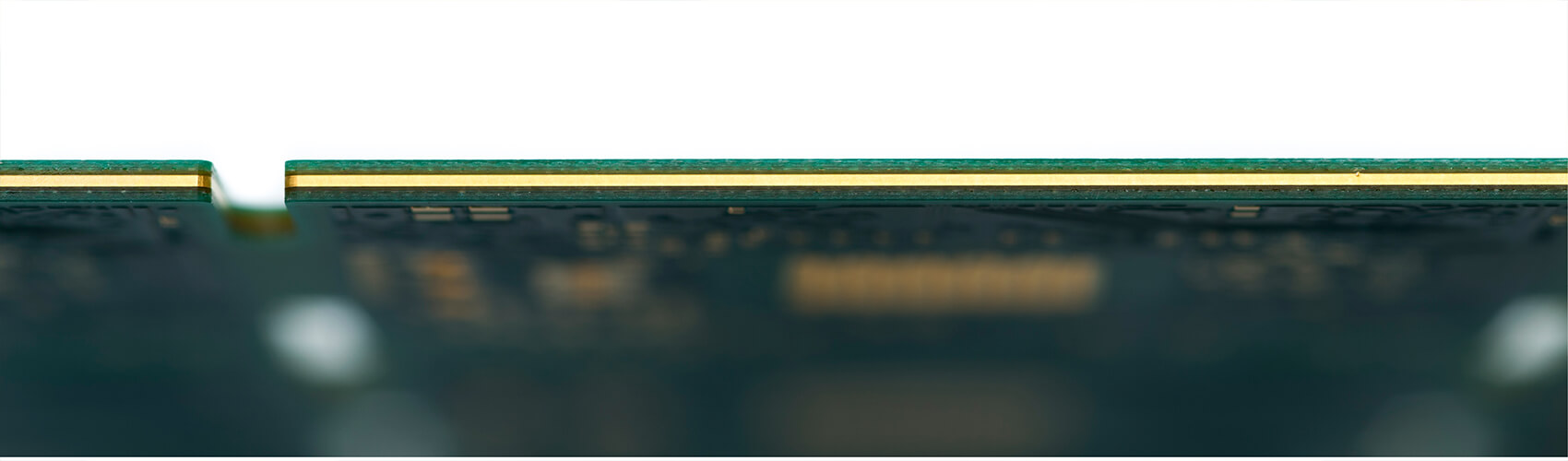
Thick Copper Technology - HiCu PCB
The Solution for Power Electronics Applications
Thick copper PCBs are traditionally used in power electronics. Thick Copper PCBs are an optimal solution used for the voltage distribution and the management of high current. Here, the thick copper can be placed both on the outer layer but also in the inner layer. If the structure of a multilayer is chosen so that the thick copper is inside, even finer structures are possible on the outer layer.
Applications:
- relay and fuse boxes, DC/DC converters
- realisation of power and signal circuits on one board
- inverters for renewable energy sources
- planar transformers
Product Range:
Unimicron Germany offers the following thick copper technologies:
- double-sided PCB up to 210 µm plated through
- multilayers with inner layer Cu up to 400 µm
- semiflex PCBs in all variations
Combinations of thick copper inner layers (IL) with HDI technology (High Density Interconnection/laser via/blind via technique) are possible.
A great advantage of the HiCu PCBs is that - with the appropriate choice of the printedcircuit board build-up - power and control electronics can be combined in one board. This can be realised by different multilayer constructions, for example: power electronics on inner layers and control electronics on outer layers.
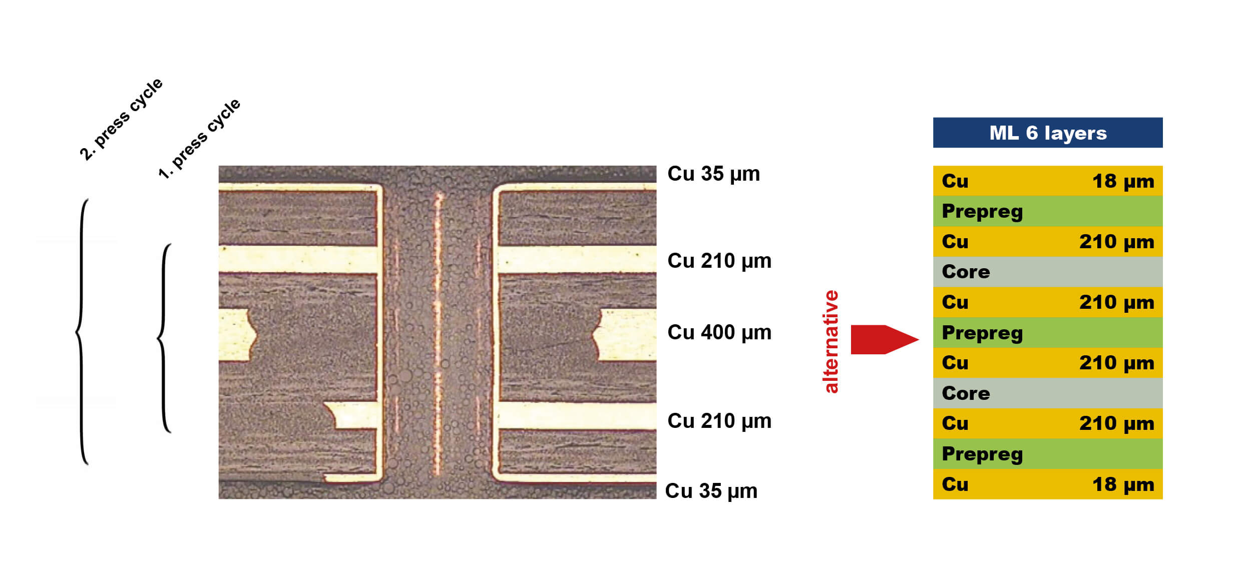
Sequential construction of a thick copper multilayer and a cost-effective alternative (example):
Base Materials
Unimicron Germany uses almost exclusively high-TG materials for these applications. This is necessitated by rising demands made of temperature stability and thermal cycling strength. As a result of the high copper thicknesses the material is subject to further, considerably higher requirements.
The base copper thicknesses used for outer and inner layers are 105 µm, 140 µm, 175 µm, 210 µm. Only for inner layers 400 µm too.
CAP Layer Technology as an Alternative for Higher Copper Thicknesses:
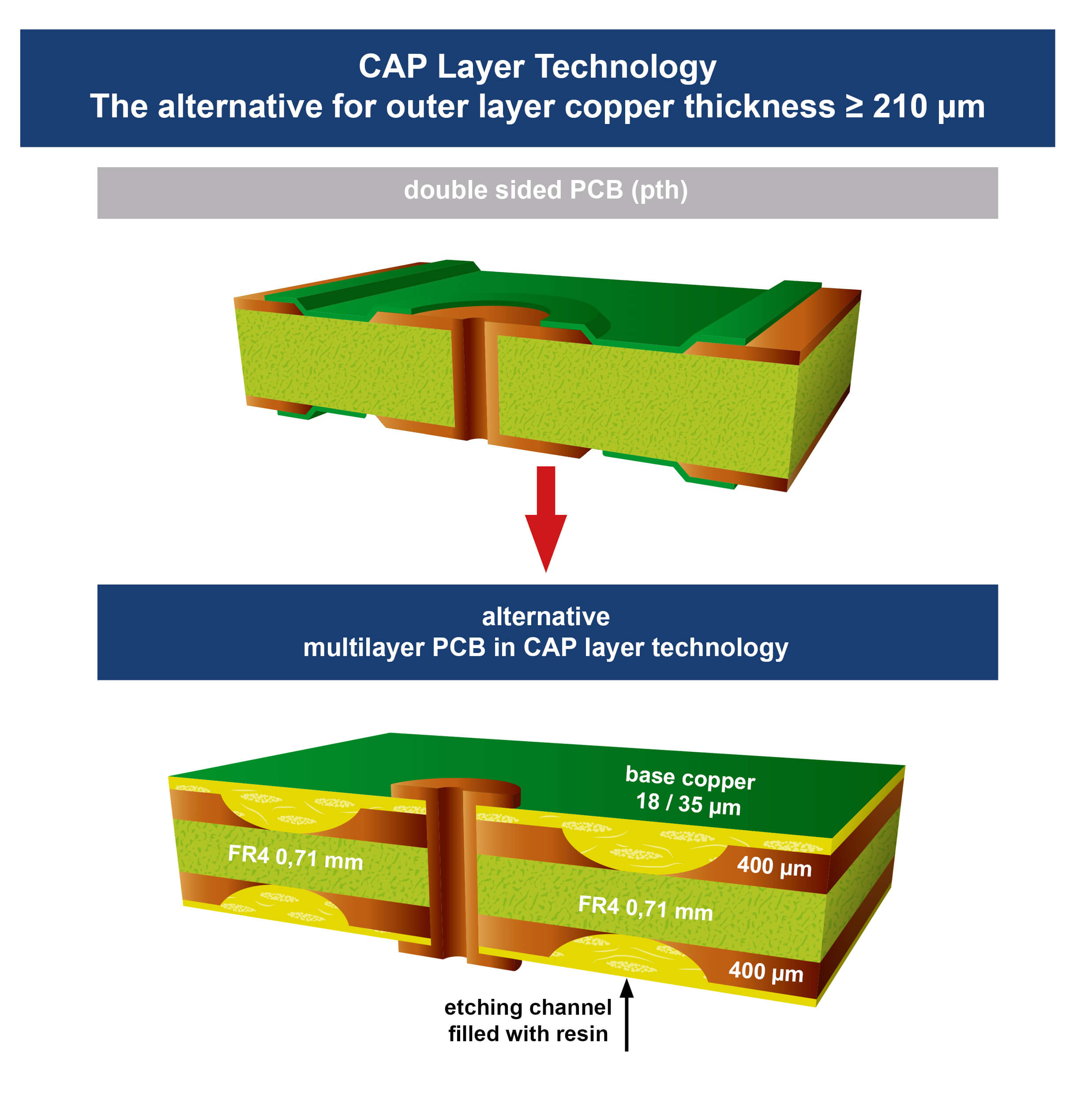
Advantages of the CAP Layer Technology:
- significantly enhanced performance in the thermal cycling test
- cost benefit and enhanced thermal resistance of the surface, solder resist can be dispensed
- “closed system” without the risk of air inclusions
- higher resistance to mechanical damages
- dependent on Cu thickness cost-neutral
Design Rules:
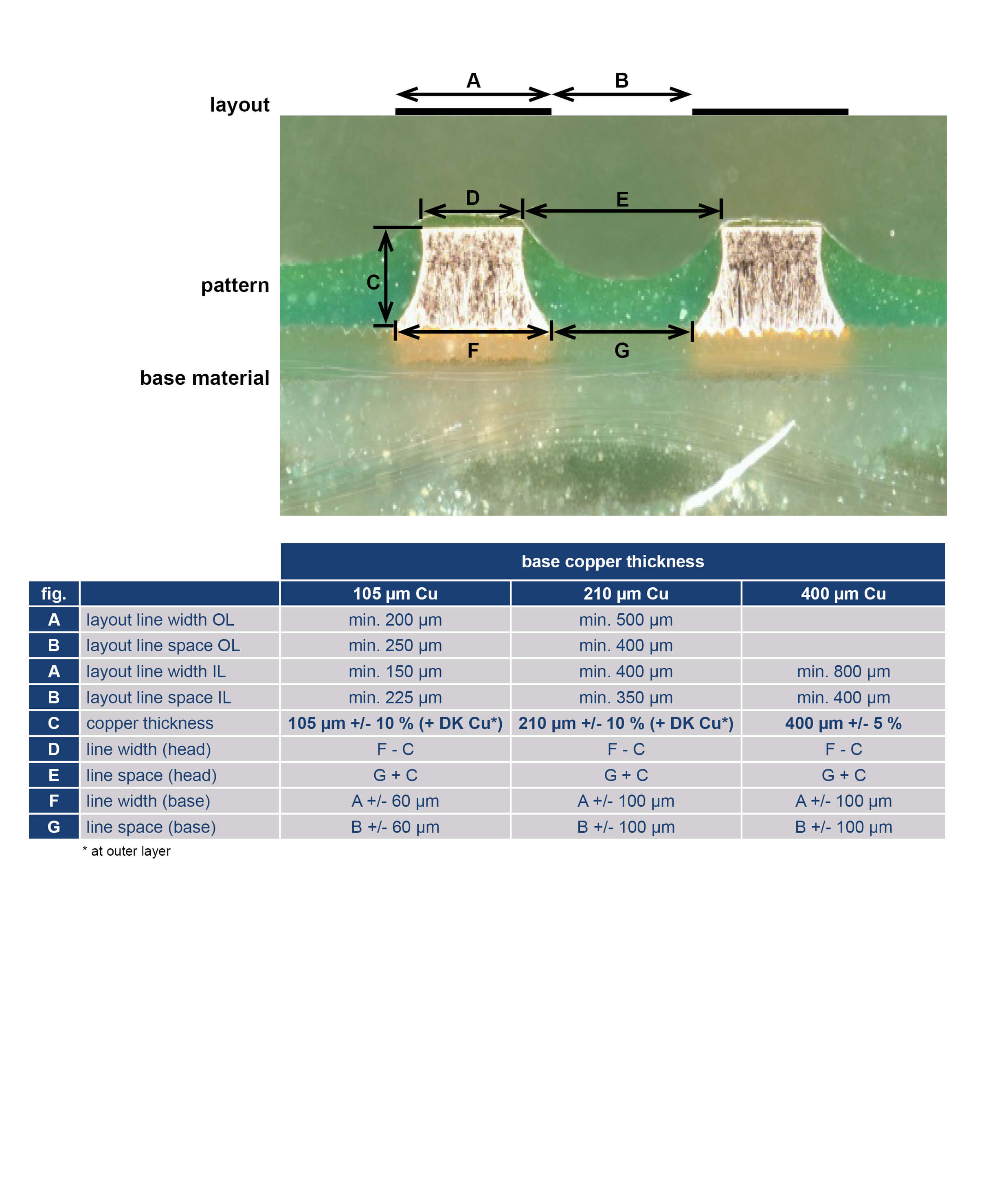
Technically realisable values, valid for inner and outer layers
Heating of Thick Copper Conductors
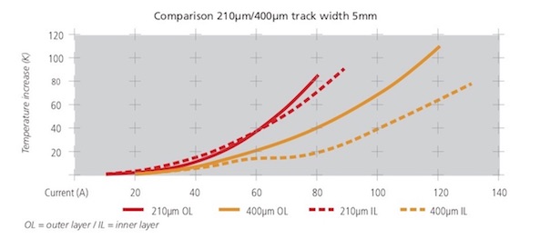
Thanks to our high current measuring station we are able to test new materials and technologies up to a maximum current intensity of 1,500 A.
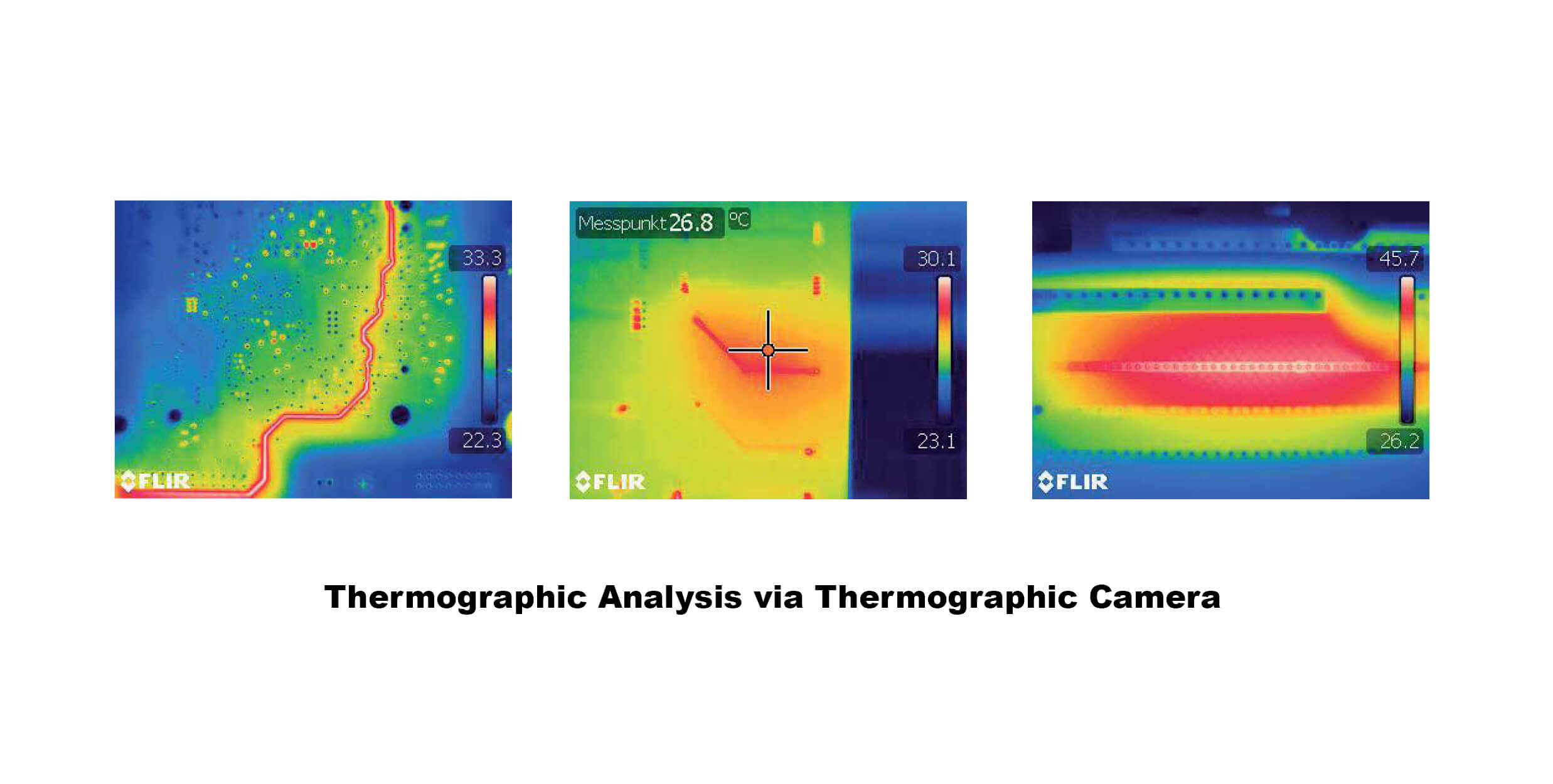
The analysis (temperature curve and distribution) is conducted using a thermographic camera.
Knowhow
- Large connected copper areas should be avoided for the layout because they may provoke mechanical tensions.
- The drilling time increases considerably due to the thick copper, i.e. special drilling parameters and drill bits must be used. This means also that higher expenditure for drilling influences the costs directly.
- It may be necessary to apply a double coating of solder resist in order to achieve sufficient edge coverage.
- For thick copper PCBs, however, applying chemical surface finishes is recommended. For this surfaces like electroless Ni/Au and especially electroless Sn are suitable, because no thermal stress arises.
- Measurements are possible in our own measuring laboratory.
We generally recommend that you contact our product management already before designing your HiCu PCB to discuss the requirements on the PCB in detail. This makes it possible to lay the foundations for an optimal and cost-efficient solution in advance.
Contact to product management:
product management
+49 (0) 2831 - 3 94-0
info@unimicron.de
Further PCB Technologies:
Thick Copper Profile - HiCu Profile PCB | HDI Technology - HiDensity PCB | High Frequency Technology - HiFrequency PCB | Metal Inlay Technology - Metal Inlay PCB | IMS & Heatsink Technology - Metal Plate PCB | Semiflex Technology - Semiflex PCB | Partial Thick Copper Technology - Wirelaid®